
Updating a connected device is usually pretty straightforward, you click a few buttons and it updates its software directly from the internet. Sweet!
However, it was not always this simple  On my good old Texas Instruments calculator, the TI-92, you have to replace a physical module to update its firmware.
Should be pretty simple, right ? You go to Amazon, search for a TI-92 module and well… Nothing 
Well, it’s not really surprising for a calc from the 90s.
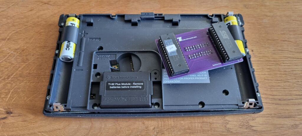
This leaves us with only one logical choice… Create our own reprogrammable ROM module! 
Reversing the module
So the first step in my journey was to reverse engineer the module to understand how it works. It was pretty straightforward to open, and inside we can see a pretty simple PCB with two MX27C4000 ROM chips. These kinds of chips are only writable once, so you can’t reprogram them to update their firmware.
Now that we have identified these two 512KB memories, we need to reconstruct the wiring to understand to which pins they connect.
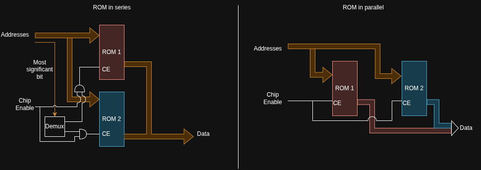
At this stage, I was pretty confident that there would be two ways of combining these ROMs: in parallel or in series 
I would just need to check a few connections using my multimeter and a pattern would appear… But oh boy, was I wrong 
Data pins were not connected between them and there was no demultiplexer, so I deduced they were in parallel. But the more I tested the connections, the less it made sense.
Generally, when you are a normal human being and connect two memories in parallel, you do something like this:
You connect the same address pins on both chips and you do that in order. And you split the data bus in half between the two chips.
But here everything was scrambled, the address pin from one chip was connected to another address pin on the other chip. The chaos present is hard to express in words, so I’ll let you admire one of my drawings trying to figure this shit out.
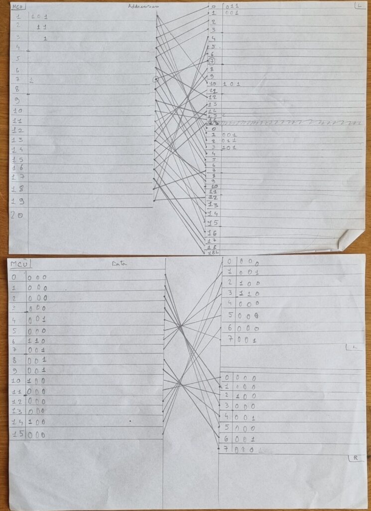
I have no idea what substance they took to make this mess, but it had to be really good 
When digging on the internet, I found a web archive documenting the TI-92 expansion module header pinout. And combining that with my reversing, I was able to figure out how it worked.
Here are some resource links in case you need them:
https://web.archive.org/web/19991012092724/http://www.daewoo.fr:80/~jjm/ti92.html
https://www.oocities.org/siliconvalley/peaks/6869
+-----+-----+-----+-----+-----+-----+-----+-----+-----+-----+-----+-----+-----+
|NC   |CE1/ |D3   |D2   |D1   |D0   |GND  |A1   |A3   |A5   |A7   |A18  |NC   |
|     |RAM  |     |     |     |     |     |     |     |     |     |     |     |
+-----+-----+-----+-----+-----+-----+-----+-----+-----+-----+-----+-----+-----+

+-----+-----+-----+-----+-----+-----+-----+-----+-----+-----+-----+-----+-----+
|Vcc  |RW/  |D11  |D10  |D9   |D8   |GND  |*    |A2   |A4   |A6   |A8   |A19  |
|RAM  |     |     |     |     |     |     |     |     |     |     |     |     |
+-----+-----+-----+-----+-----+-----+-----+-----+-----+-----+-----+-----+-----+


+-----+-----+-----+-----+-----+-----+-----+-----+-----+-----+-----+-----+-----+
|Vcc  |     |Vcc  |D12  |D13  |D14  |D15  |Vcc  |A16  |A14  |A12  |A10  |A20  |
|RAM  |     |ROM  |     |     |     |     |ROM  |     |     |     |     |     |
+-----+-----+-----+-----+-----+-----+-----+-----+-----+-----+-----+-----+-----+

+-----+-----+-----+-----+-----+-----+-----+-----+-----+-----+-----+-----+-----+
|NC   |CE2/ |D4   |D5   |D6   |D7   |GND  |A17  |A15  |A13  |A11  |A9   |NC   |
|     |RAM  |     |     |     |     |     |     |     |     |     |     |     |
+-----+-----+-----+-----+-----+-----+-----+-----+-----+-----+-----+-----+-----+

* CE/ ROM:      accesses 400000-5FFFFF on models with internal ROM,
                accesses 200000-5FFFFF on models with no internal ROM
Designing my solution
Now that it made a little more sense, I had to design my own board with modern ICs to replicate the module behaviour.
First of all, I searched for a MX27C4000 replacement and came across the SST39SF040 from Microchip with a similar pinout and timings. The main difference here is that it’s an EEPROM which means that it can be erased and rewritten electronically.
I ordered some from AliExpress, and started working on the next big part, the PCB.
The PCB
It was my first time designing a PCB, so I learned a lot
I decided to use KiCAD, as it’s open source and a reference in the field. You first start by creating a visual schematic, where you place components wherever you want and decide what connections will be made. And you then move on to the PCB layout in which you define your PCB boundaries, component placement, and trace the routes.
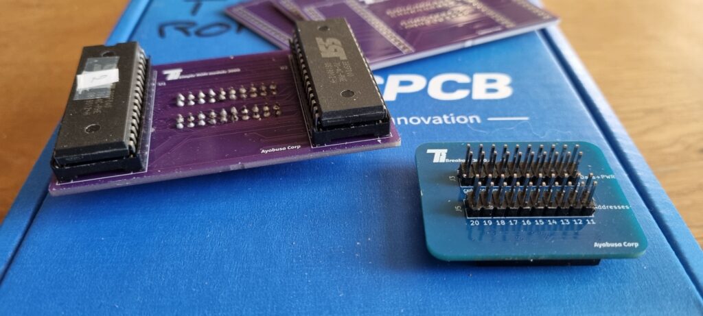
For this project, I made two boards: a small one being a breakout board, and a bigger one that sits on top and holds my two EEPROMs.
The next step was to export these boards to GERBER files and upload them to a manufacturer website, I chose JLCPCB as they are really cheap.
This process is quite fun, and I was really happy to see my design come to reality 
Creating the EEPROM programmer
I wandered around the internet to find a way to program my ROM chips, but none of the Arduino projects worked for me, and I was not ready to spend more money on a commercial programmer. So I decided to create my own using my trusty STM32 NUCLEO board.
You can find the git repo here : https://github.com/ayabusa/EEPROM-programmer
The process of creating firmware for these boards is quite smooth. ST provides tooling such as the STM32CubeMX that generates all the boilerplate code to start your project. It also provides a nice hardware abstraction layer to work with, in C.
From that point, I developed a suite of tools you could connect to through UART to interact with the Microchip EEPROM. With it, you can identify the chip, erase its content, write to it, or even dump its content. All of that was done using the chip reference manual
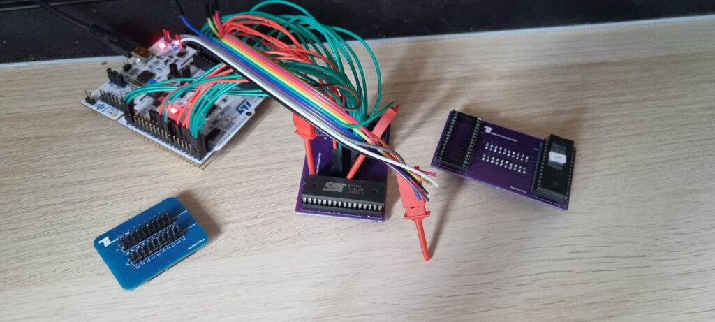
It worked great with simple tasks such as erasing the whole chip, but when it started to involve file transfers, my firmware started to fall short. I suspect it came from UART, which can be a little bit wanky sometimes. So I first started to slow down the exchange rate, which significantly improved the reliability but was still not enough. Up until this point, I simply exchanged files by dumping them as ASCII over UART. It meant that if one byte was lost, the whole binary would be shifted. So I decided to create my own file transfer protocol that would resolve both the data integrity and the shift issues.
It’s pretty simple: the sender splits the file into smaller packets and sends them to the recipient via UART. Each packet contains an address, the data, and a checksum. I wrote a PC helper in python and implemented it on the NUCLEO in C. It worked great!
UART interface:
=====================================================================================
 _____ _____ _____ _____ _____ _____
|   __|   __|  _  | __  |     |     |   ___ ___ ___ ___ ___ ___ _____ _____ ___ ___
|   __|   __|   __|    -|  |  | | | |  | . |  _| . | . |  _| .'|     |     | -_|  _|
|_____|_____|__|  |__|__|_____|_|_|_|  |  _|_| |___|_  |_| |__,|_|_|_|_|_|_|___|_|
    - Ayabusa 2026                     |_|         |___|
=====================================================================================
Hello welcome to the EEPROM programmer! What would you like to do?
[1] Dump Rom as char
[2] Erase chip
[3] Program chip via UART (Use python script)
[4] Identify device
[5] Dump Rom as file (Use python script)
Packet structure:
+---------+-----------+---------+
| Address | Data | CRC32 |
| 4 bytes | 128 bytes | 4 bytes |
+---------+-----------+---------+Final result
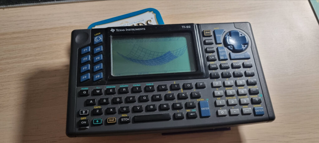
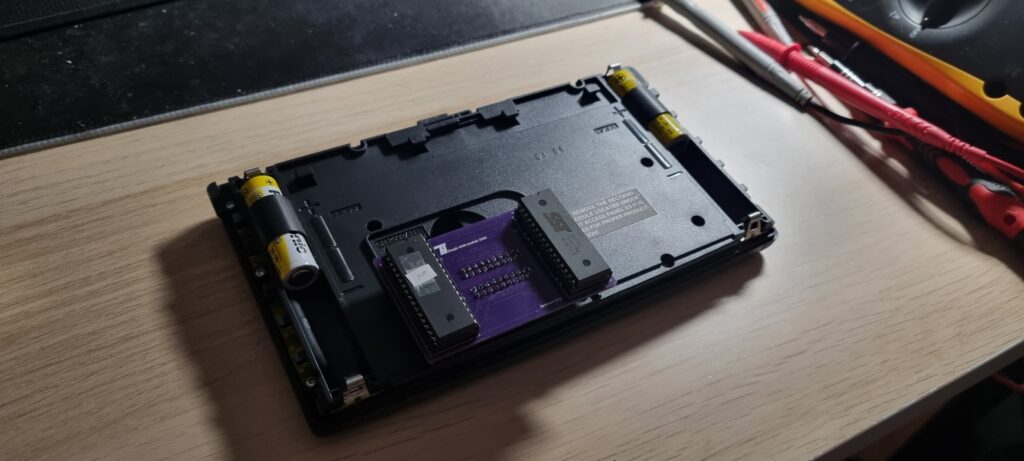
Now that everything is flashed and the PCB soldered, I just had to plug the two ROMs in (of course I swapped them at first), and IT WORKED!!! Here are some pictures running the latest ROM version possible (1.12)
Conclusion and what’s next
And that’s it for now! I’m really happy with this project. It took me a lot of time and I almost abandoned it at some point. But I’m glad the summer break gave me the opportunity to complete it, I learned a lot
As of right now it’s a good prototype, but there is still a lot to be done. First, I would like to put everything in a smaller form factor that would let me close the calc. And it would also be neat to have the ability to flash the module directly from USB.
If I manage to achieve that, I’ll be sure to write a sequel to this post. And maybe even sell it as a little product, who knows Tell me in the comments if that’s something you would like to have/build!
As always, thank you for reading my blog, it means a lot
– Ayabusa
Great job !
Dissecting, and recreating a board so that you can get features you can’t find anymore 😀
This is the way !
I wish you the best for the follow-up.
Thank you very much
Good luck on your repair !
You rock!